
Thin-Film Deposition Techniques: Physical and Chemical Methods
Thin-film deposition is a critical process in numerous industries, particularly in electronics, photonics, and material science. This technique involves the creation of thin layers of material on a substrate, and its applications range from semiconductor manufacturing to coatings for optical devices.
 [1]
[1]
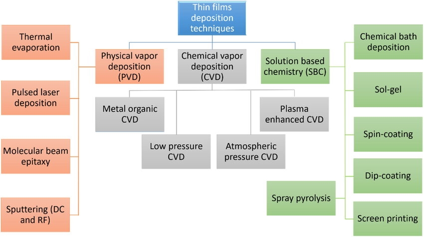
Physical Methods of Thin-Film Deposition
Physical Vapor Deposition (PVD) is one of the most widely used techniques in industry for depositing thin films. In PVD, material is vaporized from a solid or liquid phase and then condensed onto a substrate. Among the PVD methods, sputtering and evaporation are the most common.
- Sputtering involves bombarding a target material with high-energy ions, which causes atoms to be ejected and deposited on a substrate. This technique is favored for its ability to deposit films at low temperatures, which is essential for substrates that cannot withstand high heat. Sputtering is widely used in industries that require coatings with high uniformity and adhesion, such as in the production of solar cells and semiconductor devices.
- Evaporation, on the other hand, involves heating a material in a vacuum until it vaporizes. The vapor then condenses onto the substrate. Electron Beam Evaporation is a variant of this technique, where an electron beam heats the material. This method is highly effective for depositing metals and dielectrics and is commonly used for optical coatings and microelectronic devices.
Molecular Beam Epitaxy (MBE) is another powerful physical method that allows for the deposition of high-quality thin films with precise atomic layer control. In MBE, a beam of atoms or molecules is directed onto a substrate under ultra-high vacuum conditions. The ability to control the deposition rate and the material's composition makes MBE ideal for applications that require high crystalline quality, such as in the development of semiconductors and quantum devices.
Another technique, Atomic Layer Deposition (ALD), stands out for its ability to deposit extremely thin, uniform films one atomic layer at a time. This method involves alternating exposure of the substrate to different precursor gases, each reacting with the surface to deposit a monolayer of material. The atomic layer precision provided by ALD is crucial for the fabrication of devices with extremely small dimensions, such as advanced transistors and capacitors used in modern integrated circuits.
Chemical Methods of Thin-Film Deposition
In contrast to physical methods, Chemical Vapor Deposition (CVD) relies on chemical reactions to deposit materials from gaseous precursors onto a substrate. This method is versatile and can be used to deposit a wide variety of materials, from metals to insulators, and even organic compounds.
- Plasma-Enhanced CVD (PECVD) utilizes plasma to excite the precursor gases, enabling the deposition to occur at lower temperatures than traditional CVD. This makes PECVD suitable for applications involving temperature-sensitive substrates, such as polymers used in flexible electronics.
- Metal-Organic CVD (MOCVD) is another CVD variation that uses metal-organic precursors to deposit thin films, often for semiconductor applications. MOCVD is particularly effective for growing high-quality epitaxial layers, which are vital for producing light-emitting diodes (LEDs) and solar cells.
Sol-Gel Deposition is another chemical method that involves using a liquid solution to form a gel, which is then applied to a substrate. The gel undergoes a chemical reaction during heating, forming a thin film. This method is popular for applications where large-area coatings are needed, such as in the production of coatings for solar cells and optical lenses.
Electrochemical Deposition involves using electrical current to reduce metal ions from an electrolyte solution, causing the metal to deposit as a thin film on a cathode. This method is widely used in the production of metal coatings, sensors, and batteries, especially when precise control over film thickness is required.
Spray Pyrolysis is a technique where a precursor solution is sprayed onto a heated substrate. The heat causes the solution to decompose and form a thin film. This method is often used to produce thin films for sensors, solar cells, and other applications where large-scale deposition is necessary.
Choosing Between Physical and Chemical Methods
The choice between physical and chemical deposition methods depends on several factors, including the desired properties of the film, the material being deposited, the substrate, and the intended application.
- Physical methods, such as sputtering and evaporation, are ideal for high-purity films with uniform thickness, especially when the substrate cannot withstand high temperatures. These methods are often used in electronics, optics, and magnetic coatings.
- Chemical methods, on the other hand, offer more flexibility and can be used to deposit a wide range of materials, including complex compounds and multi-layer structures. These methods are typically chosen for applications requiring intricate film structures or materials with specific chemical properties, such as semiconductors, solar cells, and high-performance coatings.
Conclusion
The ongoing advancements in thin-film deposition techniques, both physical and chemical, continue to push the boundaries of what is possible in modern electronics and materials science. As industries demand more sophisticated materials with improved performance, the development of these deposition methods will remain central to the future of high-tech manufacturing. For more details, please check Stanford Electronics.
Reference:
[1] Yaseen, & Khattak, Muhammad & Khan, Abbas & Bibi, Shaista & Bououdina, Mohamed & Usman, Muhammad & Khan, Niaz & Pirzado, Azhar Ali Ayaz & Abumousa, Rasha & Humayun, Muhammad. (2023). State-of-the-art electrochromic thin films devices, fabrication techniques and applications: a review. Nanocomposites. 10. 1-40. 10.1080/20550324.2023.2291619.


 Powder for Li-ion Battery Cathodes")
