
The Evolution of Printed Circuit Boards (PCBs): The Heart of Modern Electronics
Introduction
In the world of modern electronics, Printed Circuit Boards (PCBs) are the unsung heroes that power nearly every device we rely on today. From the smartphones in our pockets to the advanced systems in aerospace and medical equipment, PCBs serve as the foundation upon which electronic components are mounted and interconnected. Over the decades, the design, materials, and manufacturing processes of PCBs have undergone remarkable transformations, enabling the creation of smaller, faster, and more efficient devices. This article explores the evolution of PCBs, their types, materials, manufacturing processes, and the future trends shaping this critical technology.
The Basics of PCBs: How They Work
At their core, PCBs are flat boards made of non-conductive materials, typically fiberglass, with conductive pathways—known as traces—etched or printed onto their surfaces. These traces connect various electronic components, such as resistors, capacitors, and integrated circuits (ICs), to form a complete electronic circuit. By providing a stable platform for these components, PCBs ensure reliable electrical connections and efficient signal transmission.
The invention of PCBs revolutionized electronics by replacing the bulky and error-prone point-to-point wiring systems of the past. Today, PCBs are indispensable in virtually every electronic device, from simple household gadgets to complex industrial machinery.
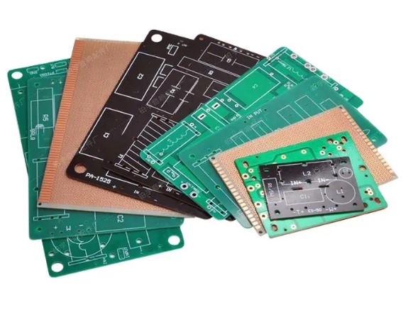
Types of PCBs: Meeting Diverse Needs
As technology has advanced, so too has the variety of PCBs available. Different applications require different types of PCBs, each with its own unique design and functionality. Here are the most common types:
1. Single-Layer PCBs: The simplest and most cost-effective type, single-layer PCBs have conductive traces on only one side of the board. They are commonly used in basic electronic devices like calculators and power supplies.
2. Double-Layer PCBs: These PCBs feature conductive traces on both sides of the board, allowing for more complex circuits. They are widely used in consumer electronics, such as LED lighting and automotive dashboards.
3. Multi-Layer PCBs: Consisting of three or more layers of conductive material separated by insulating layers, multi-layer PCBs are used in highly complex devices like smartphones, computers, and medical equipment. They offer greater design flexibility and improved performance.
4. Flexible PCBs: Made from flexible materials like polyimide, these PCBs can bend and twist without breaking. They are ideal for wearable electronics, foldable devices, and applications where space is limited.
5. Rigid-Flex PCBs: Combining the durability of rigid PCBs with the flexibility of flexible PCBs, rigid-flex PCBs are used in applications that require both strength and adaptability, such as aerospace and military systems.
Materials Used in PCBs: The Building Blocks
The materials used in PCBs play a critical role in their performance and durability. The most common material is FR-4, a flame-retardant fiberglass epoxy laminate known for its excellent mechanical and electrical properties. However, different applications require specialized materials:
- Polyimide: Used in flexible PCBs, polyimide offers high thermal stability and flexibility.
- Ceramic: Ideal for high-temperature applications, ceramic PCBs provide superior thermal conductivity and durability.
- Metal-Core PCBs: These PCBs use a metal base, such as aluminum or copper, to dissipate heat efficiently, making them suitable for high-power applications like LED lighting.
The choice of material depends on factors such as thermal conductivity, flexibility, and the operating environment of the electronic device.
The PCB Manufacturing Process: From Design to Reality
The production of PCBs is a complex and precise process that involves multiple steps. Here’s an overview of how PCBs are made:
1. Design: The process begins with the creation of a circuit design using specialized software. Engineers carefully plan the layout of components and traces to ensure optimal performance.
2. Printing: The design is transferred onto the PCB using a photolithographic process. A light-sensitive material, called a photoresist, is applied to the board, and the design is printed onto it using UV light.
3. Etching: Unwanted copper is removed from the board using a chemical solution, leaving behind the conductive traces that form the circuit.
4. Drilling: Holes are drilled into the board for component leads and vias, which connect different layers of the PCB.
5. Plating: The holes are plated with conductive material to ensure electrical connectivity between layers.
6. Solder Mask Application: A protective layer, called a solder mask, is applied to the board to prevent short circuits and protect the traces from environmental damage.
7. Silkscreen Printing: Labels, identifiers, and component outlines are printed onto the board to assist with assembly and troubleshooting.
8. Testing: The finished PCB undergoes rigorous testing to ensure it functions as intended and meets quality standards.
Conclusion
Printed Circuit Boards have come a long way since their inception, evolving from simple single-layer boards to highly sophisticated multi-layer and flexible designs. As the backbone of modern electronics, PCBs play a crucial role in enabling the devices and technologies that shape our world. Looking ahead, the continued innovation in PCB materials, manufacturing processes, and design will pave the way for even more advanced and sustainable electronic systems. Whether in consumer electronics, healthcare, or aerospace, the future of PCBs is bright—and their evolution is far from over. For more LCD basics, please check Stanford Electronics.

: The Heart of Modern Electronics")
: An Overview")
